During the coffee break this morning, I added two new pages to my Excel calculator.
The first is the 6.1 table (IPC2221) gives the spacing for a given voltage.
The second helps to move a component. For a given target, ie the desired position of a pin of a component, you indicated the current position of the object, and the position of the connected component, and you get the new position of the component.
I invented nothing here, I try to put all my tricks in a single file. This way when I lose the file, I lose them all simultaneously. :-)
PCB_Design_Claculator.zip
Thursday, February 26, 2015
Monday, February 16, 2015
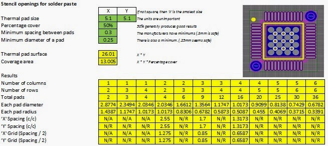
Solder paste openings for thermal pads
Hi,
Minus 23°C this morning. Such a nice day to add a page to my calculator...
Drawing solder paste openings for thermal pads is always a compromise.
First, to prevent the slides of components in the weld, everyone agrees that the solder paste should cover about 50% of the pad.
Second, we know that large solder paste surface favors the creation of voids. We prefer an array of small areas.
Third, my assemblers friends prefer round openings, which are easier to clean.
We must also take into account the space between the openings, even laser cut, the material used for stencils has its limits.
In addition, it is often necessary to add vias in the pad for improved thermal conduction. Then we'd rather have filled vias, but the filling has a cost, and it is often desired without.
The vias are surely necessary to heat conduction, but if the component is not welded, conduction will not happen.
So I added a page to my calculator that allows to reach an interesting pattern. Subsequently we have to find the right size, quantity and dispersion of vias. Vias not too big, located between the solder paste openings should minimize leakage of solder in the holes. But I was not able to meet the specification everyone, and the result is a compromise.

Thursday, February 12, 2015
Land Requirements
To start the day, add a page to our Excel calculator.
This morning we automates the calculations for Land Requirements, following the IPC-2221 Generic Standard on Printed specification Board Design.
To calculate the size of the pads of our vias according to the Producibility Level.
PCB_Design_Claculator.zip
This morning we automates the calculations for Land Requirements, following the IPC-2221 Generic Standard on Printed specification Board Design.
To calculate the size of the pads of our vias according to the Producibility Level.
PCB_Design_Claculator.zip
Wednesday, February 11, 2015
V-Groove Scoring Calculator
A few days off, and as it's been a while since I wrote something here do, and I'm a little lack of novelty, so here's a new calculator.
This first (hopefully) version allows to calculate the distance to be maintained between the edge of the PCB and copper or components when a V-Scoring is used to separate the PCBs after panelization.
http://bit.ly/1AXGgBE
This first (hopefully) version allows to calculate the distance to be maintained between the edge of the PCB and copper or components when a V-Scoring is used to separate the PCBs after panelization.
http://bit.ly/1AXGgBE
Wednesday, August 29, 2012
ODB++ Solutions Alliance
ODB++ Solutions Alliance:
Looking for a source of information about the format ODB + +? The ODB + + Solutions Alliance is not only a good start, it could also be the end of your search.
Register for free and get access to all resources.
'via Blog this'
Looking for a source of information about the format ODB + +? The ODB + + Solutions Alliance is not only a good start, it could also be the end of your search.
Register for free and get access to all resources.
'via Blog this'
Monday, August 6, 2012
PCB Libraries
Good news
For those who do not have the business volume to justify paying a tool, and for those who like well done job, PCB libraries is back online with their new tool Footprint Expert 2012.
Welcome back Tom.
Thursday, March 22, 2012
Subscribe to:
Posts (Atom)